Beyond GPUs: How Broadcom Custom Silicon Is Reshaping AI Infrastructure
Broadcom is building the custom silicon backbone behind Google, Meta, OpenAI, Apple, Anthropic, ByteDance, and Fujitsu. Here is how XPUs work, why they are increasingly attractive for large-scale inference, and what NVIDIA's NVLink Fusion response means for the future of AI compute.
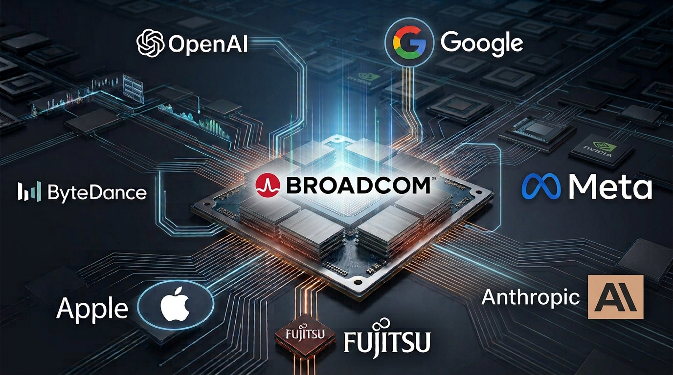
There is a quiet shift happening in AI infrastructure. While everyone watches NVIDIA's quarterly earnings and GPU supply chain, Broadcom is building the custom silicon that powers some of the largest AI deployments on the planet. Google's TPUs, Meta's MTIA chips, OpenAI's Jalapeno processor, Apple's Baltra server chips, Anthropic's inference backbone, ByteDance's recommendation engines, and Fujitsu's next-generation supercomputer all run on Broadcom-designed XPUs. That is not a side business. That is $17 billion in annualized revenue and growing [1].
What Is an XPU and Why It Matters
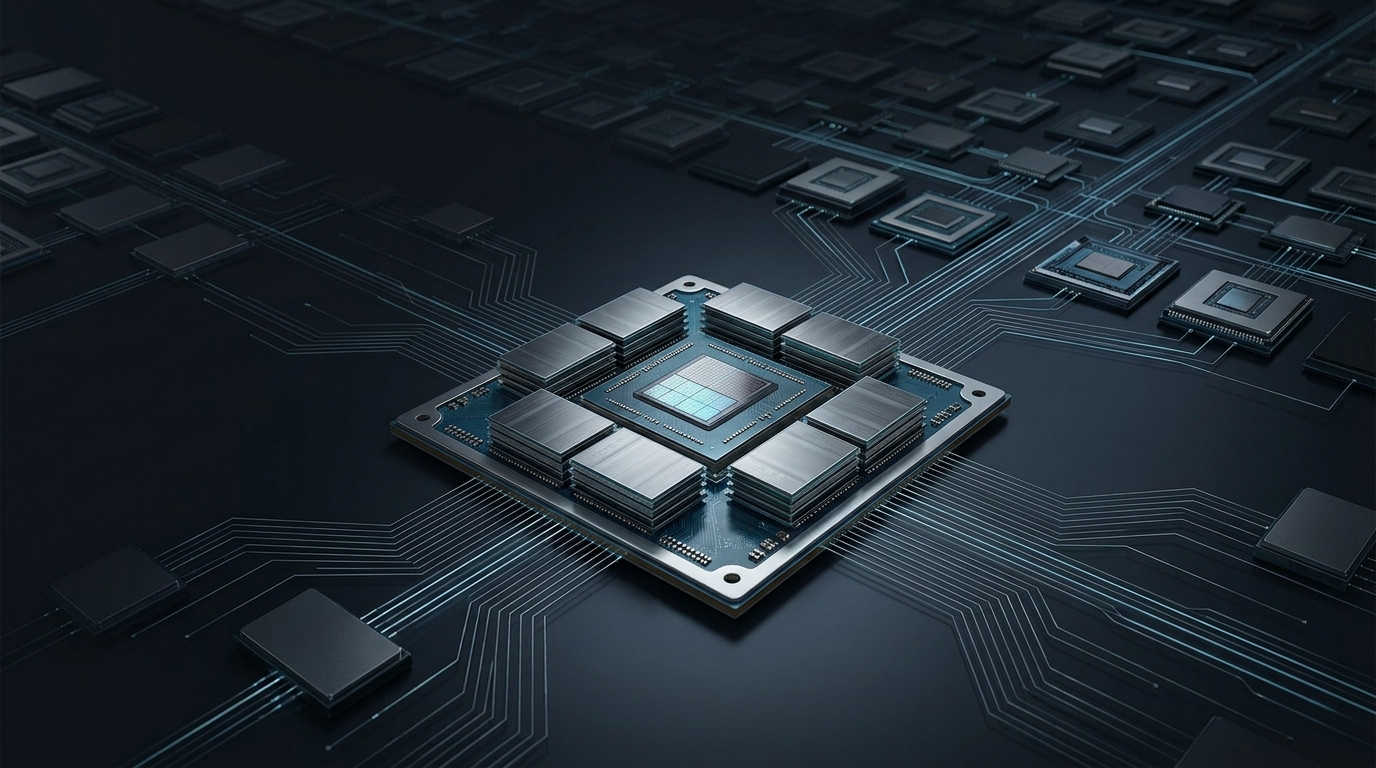
An XPU is a custom-designed accelerator chip, built specifically for one customer's workload. Unlike a GPU, which is a general-purpose processor designed to run any AI model, an XPU is optimized for a narrow set of tasks. Think of it this way: a GPU is a Swiss Army knife. An XPU is a scalpel.
The difference shows up in production. For highly optimized workloads, custom accelerators can deliver substantially better performance per watt than general-purpose GPUs, although the actual advantage depends on workload characteristics, model architecture, precision, memory behavior, and system design. Google, for example, claims its Ironwood TPU achieves roughly 44% lower total cost of ownership than a comparable NVIDIA GB200 server, according to SemiAnalysis modeling of Google's internal cost structure [2].
This is the core reason hyperscalers are investing in custom silicon. Training a frontier model still demands the raw flexibility of GPUs and NVIDIA's CUDA ecosystem. But once that model is trained, serving it to hundreds of millions of users is pure inference. And inference is where the economics are decided. As AI moves from model development into production, inference becomes the dominant recurring infrastructure cost. That changes the optimization target from peak compute to cost per query, latency, utilization, and performance per watt. The cheaper you can run inference, the wider your margins on every API call, every chat response, every generated image. At hyperscale, that efficiency gap decides who can afford to offer AI at a price the market will pay. That is exactly where custom XPUs provide a significant advantage.
The Real Bottleneck Is Not Always Compute
Before diving into partnerships, it is worth understanding why custom silicon can outperform general-purpose GPUs for inference workloads. The answer is not just raw TFLOPS.
In LLM inference, the bottleneck is often memory bandwidth, not compute. A model's weights must be loaded from HBM into the compute units for every token generated. The KV cache grows with sequence length and batch size. Data moves constantly between memory, compute, and network interfaces.
A general-purpose GPU optimizes for peak FP operations across a wide range of workloads. A custom XPU can optimize the entire data path: memory hierarchy, HBM interfaces, data movement patterns, interconnect topology, numerical precision, sparsity handling, and scheduling. When you control the full stack from silicon to software, you can eliminate bottlenecks that a general-purpose architecture must tolerate.
This connects directly to Broadcom's 3.5D XDSiP packaging (covered below) and NVIDIA's NVHBM response: both are fundamentally about reducing the memory wall, not adding more ALUs.
Who Is Building With Broadcom
Broadcom's XPU customer list reads like a who's-who of AI. Each partnership illustrates a different facet of why custom silicon is gaining traction.
Google is the anchor partner and the longest relationship, going back to 2014 across seven TPU generations. The latest Ironwood TPU delivers 4,614 FP8 TFLOPS per chip with 192 GB of HBM3E memory [2]. A single 9,216-chip superpod produces 42.5 exaflops of compute. According to analyst estimates, Google accounts for the majority of Broadcom's XPU revenue.
Meta is the second-largest XPU customer by revenue share. In April 2026, Meta and Broadcom announced a partnership to co-develop multiple generations of MTIA (Meta Training and Inference Accelerator) chips, with an initial commitment exceeding 1 GW [3][4]. Meta's roadmap is aggressive: four new MTIA generations (300 through 500) announced in early 2026, with the MTIA 500 targeting 10 PFLOPS FP8 and 512 GB HBM by 2027. From MTIA 300 to 500, HBM bandwidth increases 4.5x and compute scales 25x. Meta's approach is pragmatic. They use NVIDIA GPUs for frontier model training and MTIA silicon for optimized inference across Facebook, Instagram, and their generative AI products. As Mark Zuckerberg put it: "This partnership will give us greater performance and efficiency for everything we're building."
OpenAI: From Model to Silicon
The OpenAI partnership is perhaps the clearest illustration of how custom silicon development works in practice. The pipeline looks like this:
Frontier models → workload analysis → architecture design → custom accelerator → networking integration → hyperscale deployment
OpenAI signed a strategic collaboration with Broadcom to deploy 10 gigawatts of custom AI accelerators and Ethernet networking solutions, with deployment beginning in the second half of 2026 and running through 2029 [5][6]. The first product is Jalapeno, OpenAI's first Intelligence Processor.
Jalapeno was purpose-built for LLM inference, designed from scratch rather than adapted from general-purpose architectures. The chip reportedly went from design to manufacturing tape-out in approximately nine months [6]. Engineering samples are already running production workloads, including GPT-5.3-Codex-Spark, at target frequency and power.
What makes this significant is not just the chip itself, but the integration. Jalapeno incorporates Broadcom's silicon implementation and Tomahawk networking technologies, with Celestica handling board, rack, and system integration. OpenAI president Greg Brockman called it "part of our long-term full-stack infrastructure strategy to make compute more abundant." Broadcom CEO Hock Tan added: "This is just the beginning of a multi-generation roadmap."
This is a pattern worth watching: an AI company designs its workload-specific accelerator, Broadcom implements the silicon and networking, and the result deploys at gigawatt scale.
Apple extended its Broadcom partnership through 2031. Broadcom will develop custom ASICs for Apple's AI server infrastructure, specifically for upcoming dedicated chips codenamed Baltra, scheduled for deployment in 2027 [7]. These chips will power Apple Intelligence features including advanced text and image generation, optimizing Apple's data centers for inference workloads.
Anthropic is positioned to become one of Broadcom's largest XPU customers in the coming years. Through the AI XPV platform, a joint venture backed by $35 billion from Apollo Global Management and Blackstone [8][9], Anthropic will receive an initial 1 GW deployment starting mid-2026. The partnership has outlined plans to scale toward 5 GW and eventually 10 GW, though the exact timeline will depend on deployment readiness and demand. Anthropic is also building an in-house chip design team and exploring a separate custom chip co-designed with Samsung, using Samsung's zHBM technology that places memory directly atop logic cores.
ByteDance runs custom recommendation ASICs for TikTok's infrastructure through Broadcom's XPU platform.
Fujitsu received Broadcom's first 2nm compute SoC, built on the 3.5D XDSiP platform, for the FugakuNEXT supercomputer launching in 2027 [1].
Management targets expanding to eight customers by FY2027, with potential additions including Microsoft and Amazon.
The Engineering Edge: 3.5D XDSiP
The technology behind Broadcom's XPU position is its 3.5D eXtreme Dimension System in Package (XDSiP) platform [1]. Traditional chip packaging places chiplets side by side on a substrate (2.5D). Broadcom's approach stacks them face to face, with active circuitry oriented inward toward each other.
The platform supports over 6,000 mm² of silicon, more than double the 2,500 mm² possible with 2.5D approaches. It accommodates up to 12 HBM stacks instead of the previous limit of 8. Shorter signal distances reduce both latency and power consumption, directly addressing the memory bandwidth bottleneck discussed earlier.
In February 2026, Broadcom began shipping its first 2nm compute SoC on this platform, an industry first [1].
The Networking Backbone
Building fast chips means little if you cannot connect them efficiently. This is where Broadcom's networking heritage adds a layer that pure chip designers typically lack.
Tomahawk 6 is the world's first 102.4 Tbps Ethernet switch chip, doubling current market capacity in a single device [2]. It supports 1,024 ports at 100G SerDes, with Cognitive Routing 2.0 providing advanced telemetry, dynamic congestion control, and adaptive flow control tailored to mixture-of-experts, fine-tuning, and reinforcement learning workloads. In a two-tier configuration, it scales to over 100,000 XPUs at 200 Gbps per link. Partners including AMD, Arista, Juniper, and Supermicro are integrating the technology. The upcoming Tomahawk 7, already taped out at 204.8 Tbps, pushes further.
Jericho 4, the 51.2 Tbps fabric chip, enables interconnecting over one million XPUs across data centers. The Jericho line carries a story worth telling. It originated from Dune Networks, an Israeli startup based in Yakum that developed scalable interconnect fabric technology for data centers. Broadcom acquired Dune in 2009 for $178 million, and the Jericho name was kept as a tribute to the team and innovation that came from Israel. Today, Jericho chips power the high-end chassis of Arista, Cisco, HPE, Juniper, and Nokia, forming the backbone fabric of the world's largest networks.
Broadcom is also an active contributor to MRC (Multipath Reliable Connection), an open networking protocol developed alongside OpenAI, AMD, Microsoft, and Intel [10][11]. MRC redesigns Ethernet transport for large-scale AI training clusters, addressing the congestion and reliability challenges that emerge when tens of thousands of accelerators need to communicate simultaneously. AMD has contributed its advanced congestion control technology from the Pensando Pollara 400 AI NIC [11], and the protocol has already been validated at scale in production test clusters.
The combination of custom compute, advanced packaging, and Ethernet networking gives Broadcom exposure to multiple layers of the AI infrastructure stack.
The Financial Picture
Broadcom's AI-related revenue hit $16.74 billion in Q3 FY2026, growing 3.2x year over year [1]. Of that, $12.22 billion came from AI compute (primarily XPUs) and $4.52 billion from AI networking. The company targets AI chip revenue exceeding $100 billion by 2027.
The cost structure tends to favor custom silicon at hyperscale. Based on analyst models and management commentary, custom XPU systems are estimated at approximately $12-15 billion per gigawatt of compute capacity, including CPUs and infrastructure. For comparison, NVIDIA's Grace-Hopper is estimated at roughly $18 billion per gigawatt, with the next-generation Vera-Rubin platform climbing to approximately $40 billion per gigawatt. These figures depend on configuration, utilization assumptions, and what is included in the total cost, so they should be treated as directional rather than absolute. Still, at multi-gigawatt scale, even modest per-GW savings compound into significant capital differences.
Custom ASIC-based AI server shipments are projected to reach 27.8% of the market in 2026, with ASIC shipments growing substantially faster than merchant GPU shipments year over year.
Why GPUs Are Not Going Away
It would be a mistake to read this as "GPUs are dead." They are not. The shift is toward heterogeneous infrastructure, not replacement.
| Workload | GPU | Custom XPU |
|---|---|---|
| Frontier model training | Strong fit | Limited |
| Rapidly changing models | Strong fit (flexibility) | Longer redesign cycles |
| Large-scale stable inference | Flexible but general-purpose | Highly optimized |
| Performance per watt | General-purpose baseline | Potentially significant gains |
| Software ecosystem | CUDA advantage | Customer-specific stack |
| Time to deployment | Faster | Longer design cycle |
| Volume economics | Good | Can be excellent at scale |
The key insight is that an XPU is not a "better GPU." It is a trade-off. You give up flexibility to gain optimization. That trade-off makes sense when your workload is stable, your scale is massive, and your inference costs are your largest infrastructure expense. For research, experimentation, and rapidly evolving model architectures, GPUs remain the practical choice.
NVIDIA's Response: NVLink Fusion
NVIDIA's response to the custom silicon trend is NVLink Fusion [9]. Rather than forcing customers to choose between custom accelerators and NVIDIA infrastructure, it provides a path for custom XPUs to participate in the NVIDIA scale-up ecosystem.
NVLink Fusion is a chiplet-based bridge that connects custom XPUs to NVIDIA's NVLink fabric, enabling heterogeneous racks where custom accelerators sit alongside NVIDIA GPUs, CPUs, and networking. Partners including MediaTek and d-Matrix are already building NVLink Fusion-compatible XPUs.
The architecture requires that each NVLink Fusion rack includes at least one NVIDIA component, whether a Vera CPU, ConnectX NIC, BlueField DPU, or Spectrum-X switch. This creates a model where custom silicon adoption still generates NVIDIA revenue at the rack level.
NVIDIA is also introducing NVHBM, a custom memory base-die technology offering up to 30% more bandwidth, 67% less PHY area, and 15% lower power consumption compared to standard HBM4e, translating to approximately 25% more compute-die area and roughly 15,000 additional XPUs per gigawatt of data center capacity [9]. This directly targets the memory bottleneck that drives XPU adoption in the first place.
The trade-off for customers is clear: NVLink Fusion offers integration with NVIDIA's proven software ecosystem and supply chain, while independent Ethernet-based architectures (using Broadcom's Tomahawk and Jericho) offer more flexibility and potentially lower cost at scale.
What This Really Means
The more important shift is not from GPUs to XPUs, but from homogeneous AI infrastructure to heterogeneous architectures. GPUs remain critical for flexibility and frontier training, while custom XPUs are increasingly taking over workloads where scale, efficiency, and predictable economics matter most.
Broadcom occupies an unusual position in this transition, combining custom compute design, advanced packaging, high-bandwidth memory integration, Ethernet switching, and AI networking across several layers of the infrastructure stack.
The result is a different way of thinking about AI infrastructure: not a single accelerator, but an integrated system in which compute, memory, and networking are designed together for specific workloads at specific scales.
The real competition is no longer simply GPU versus XPU. It is who can integrate compute, memory, networking, and software into the most efficient AI system. And that competition is just getting started.
References
[1] Broadcom Ships 3.5D Face-to-Face Compute SoC Powering AI Revolution↗ - Broadcom [2] Broadcom Ships Tomahawk 6: World's First 102.4 Tbps Switch↗ - Broadcom [3] Meta Partners With Broadcom to Co-Develop Custom AI Silicon↗ - Meta [4] Broadcom Announces Extended Partnership with Meta↗ - Broadcom [5] OpenAI and Broadcom Announce Strategic Collaboration to Deploy 10 Gigawatts of AI Accelerators↗ - Broadcom [6] OpenAI and Broadcom Unveil LLM-Optimized Intelligence Processor↗ - OpenAI [7] Apple, Broadcom Extend Custom AI Chip Partnership Through 2031↗ - MacDailyNews [8] Anthropic Reveals Plan to Develop Custom Chip↗ - SiliconANGLE [9] NVIDIA NVLink Fusion Brings NVHBM to Next-Generation AI Infrastructure↗ - NVIDIA [10] MRC: The Journey from Concept to Open Specification↗ - Broadcom [11] AMD Advances AI Networking at Scale with MRC↗ - AMD [12] Broadcom, Apollo, and Blackstone Launch 20GW XPU Platform↗ - DCD
Disclosure: The author is an employee of Broadcom. This article represents the author's technical analysis and does not represent Broadcom's official position.
Discussion
No comments yet. Be the first to start the discussion.